| CPC H01L 23/49568 (2013.01) [H01L 23/3107 (2013.01); H01L 23/4952 (2013.01); H01L 23/49503 (2013.01); H01L 23/49575 (2013.01); H01L 24/48 (2013.01); H01L 24/49 (2013.01); H01L 2924/181 (2013.01)] | 8 Claims |
|
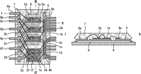
1. A semiconductor package comprising:
a plurality of die pads;
a plurality of semiconductor chips provided on the plurality of die pads respectively;
a plurality of lead terminals connected to the plurality of semiconductor chips respectively; and
a package sealing the plurality of die pads, the plurality of semiconductor chips, and the plurality of lead terminals,
the plurality of die pads and the plurality of lead terminals are exposed from a lower surface of the package, and
on the lower surface of the package, grooves are provided among the die pads adjacent to one another and among the lead terminals adjacent to one another, and the grooves are respectively spaced from the lead terminals and the die pads in a top view from one end to another end of each groove.
|