| CPC H01L 23/3185 (2013.01) [H01L 21/56 (2013.01); H01L 24/02 (2013.01); H01L 24/13 (2013.01); H01L 24/16 (2013.01); H01L 24/81 (2013.01); H01L 2224/02377 (2013.01); H01L 2224/03462 (2013.01); H01L 2224/0401 (2013.01); H01L 2224/05008 (2013.01); H01L 2224/05548 (2013.01); H01L 2224/05569 (2013.01); H01L 2224/10126 (2013.01); H01L 2224/1132 (2013.01); H01L 2224/11334 (2013.01); H01L 2224/11849 (2013.01); H01L 2224/13022 (2013.01); H01L 2224/13023 (2013.01); H01L 2224/13024 (2013.01); H01L 2224/16227 (2013.01); H01L 2224/16238 (2013.01); H01L 2224/81815 (2013.01); H01L 2224/94 (2013.01); H01L 2924/10156 (2013.01); H01L 2924/3512 (2013.01)] | 20 Claims |
|
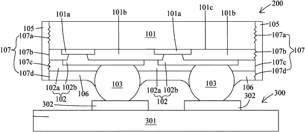
1. A method of manufacturing a semiconductor structure, comprising:
receiving a substrate;
forming an RDL over the substrate;
cutting along a sidewall of the semiconductor structure to form a plurality of recesses over a portion of the sidewall of the semiconductor structure; and
disposing an isolation layer to surround the substrate and the RDL and to extend from a level of a top surface of the RDL to a level of a bottom surface of the substrate;
wherein the cutting along the sidewall of the semiconductor structure to form the plurality of recesses over the portion of the sidewall of the semiconductor structure is performed prior to the disposing the isolation layer.
|