| CPC H01L 23/3135 (2013.01) [H01L 23/3128 (2013.01); H01L 23/49816 (2013.01); H01L 24/24 (2013.01); H01L 24/25 (2013.01); H01L 24/73 (2013.01); H01L 24/92 (2013.01); H01L 25/0657 (2013.01); H01L 25/18 (2013.01); H01L 2224/24146 (2013.01); H01L 2224/24175 (2013.01); H01L 2224/24265 (2013.01); H01L 2224/25171 (2013.01); H01L 2224/73267 (2013.01); H01L 2224/92244 (2013.01); H01L 2225/06517 (2013.01); H01L 2225/06524 (2013.01); H01L 2225/06548 (2013.01); H01L 2225/06572 (2013.01)] | 15 Claims |
|
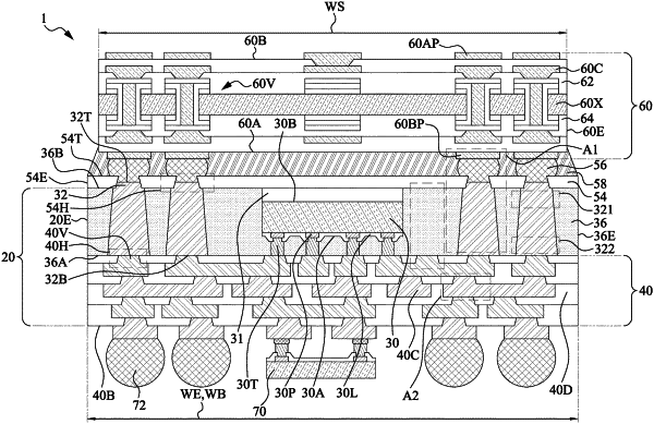
1. An electronic device package, comprising:
an encapsulated electronic component, comprising:
a redistribution layer (RDL); and
an encapsulation layer including a first surface and a second surface opposite to the first surface, wherein the first surface is closer to the RDL than the second surface is;
a substrate disposed on the second surface of the encapsulation layer;
a conductor disposed between the substrate and the encapsulated electronic component, and electrically connecting the substrate to the encapsulated electronic component; and
a buffer layer disposed between the substrate and the encapsulated electronic component and around the conductor,
wherein the buffer layer includes a first opening for the conductor electrically connecting the encapsulated electronic component, and the first opening has a first aperture having a first width, and a second aperture having a second width, the first aperture is closer to the substrate than the second aperture is, and the second width is larger than the first width.
|