| CPC H01L 21/823807 (2013.01) [H01L 21/02532 (2013.01); H01L 21/02603 (2013.01); H01L 21/823814 (2013.01); H01L 21/823821 (2013.01); H01L 21/823842 (2013.01); H01L 27/092 (2013.01); H01L 27/0924 (2013.01); H01L 29/0665 (2013.01); H01L 29/42392 (2013.01); H01L 29/66439 (2013.01); H01L 29/66545 (2013.01); H01L 29/775 (2013.01); H01L 29/78696 (2013.01); H01L 29/6681 (2013.01)] | 20 Claims |
|
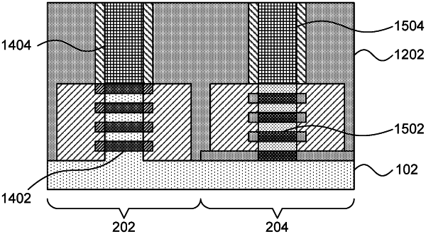
1. A nanosheet semiconductor structure comprising:
a first device, comprising:
a first plurality of vertically arranged channel layers, each channel layer of the first plurality comprising a first channel material;
a first gate structure having first gate portions, each first gate portion comprising an n-type work function metal layer, wherein the first gate portions are interleaved between successive channel layers of the first plurality of vertically arranged channel layers;
first layer caps disposed at ends of the first gate portions; and
monolithic n-type source and drain regions respectively disposed:
at opposite sides of the first gate structure; and
vertically adjacent to the corresponding first layer caps; and
a second device within the nanosheet semiconductor structure, the second device comprising:
a second plurality of vertically arranged channel layers, each channel layer of the second plurality comprising a second channel material;
a second gate structure having second gate portions, each second gate portion comprising a p-type work function metal layer, wherein the second gate portions are interleaved between successive channel layers of the second plurality of vertically arranged channel layers;
second layer caps disposed at ends of the second gate portions; and
monolithic p-type source and drain regions respectively disposed:
at opposite sides of the second gate structure; and
vertically adjacent to the corresponding second layer caps;
wherein the channel layers of the first plurality of vertically arranged channel layers are aligned horizontally with the second gate portions of the second gate structure;
wherein the monolithic n-type source region extends horizontally past each vertical outermost surface of the corresponding first layer caps to contact each of the first plurality of vertically arranged channel layers;
wherein the monolithic n-type drain region extends horizontally past each vertical outermost surface of the corresponding first layer caps to contact each of the first plurality of vertically arranged channel layers;
wherein the monolithic p-type source region extends horizontally past each vertical outermost surface of the corresponding second layer caps to contact each of the second plurality of vertically arranged channel layers; and
wherein the monolithic p-type drain region extends horizontally past each vertical outermost surface of the corresponding second layer caps to contact each of the second plurality of vertically arranged channel layers.
|