| CPC H01L 21/76898 (2013.01) [H01L 21/31105 (2013.01); H01L 21/762 (2013.01); H01L 21/76811 (2013.01); H01L 27/0629 (2013.01); H01L 28/24 (2013.01)] | 20 Claims |
|
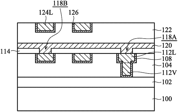
1. A semiconductor device structure, comprising:
a substrate;
a first dielectric layer over the substrate;
a first conductive feature and a second conductive feature surrounded by the first dielectric layer;
a second dielectric layer over the first dielectric layer;
a resistive element having a first portion over the second dielectric layer and a second portion penetrating through the second dielectric layer to be electrically connected to the first conductive feature; and
a conductive via penetrating through the second dielectric layer to be electrically connected to the second conductive feature, wherein the second portion of the resistive element is wider than the conductive via.
|