| CPC H01L 21/76847 (2013.01) [H01L 21/32134 (2013.01); H01L 21/76846 (2013.01); H01L 23/485 (2013.01); H01L 23/53223 (2013.01); H01L 23/53238 (2013.01); H01L 23/53252 (2013.01); H01L 23/53266 (2013.01)] | 20 Claims |
|
1. A semiconductor device comprising:
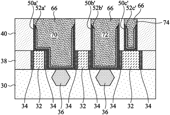
a dielectric layer over a conductive feature, the dielectric layer being a single dielectric layer, the dielectric layer having a sidewall;
a conductive layer in the dielectric layer, the conductive layer being in electrical contact with the conductive feature, wherein an upper surface of the conductive layer is level with an upper surface of the dielectric layer;
a barrier layer interposed between the conductive layer and the dielectric layer along a line parallel to the upper surface of the dielectric layer, an upper surface of the barrier layer being covered by the conductive layer, wherein a thickness of an upper portion of the barrier layer is less than a thickness of a lower portion of the barrier layer, wherein the barrier layer is a conductive material;
an adhesion layer interposed between the barrier layer and the dielectric layer; and
a gate structure and a spacer adjacent the gate structure, wherein a surface of the adhesion layer contacts a surface of the spacer.
|