| CPC H01L 21/76283 (2013.01) [H01L 21/743 (2013.01); H01L 23/535 (2013.01)] | 20 Claims |
|
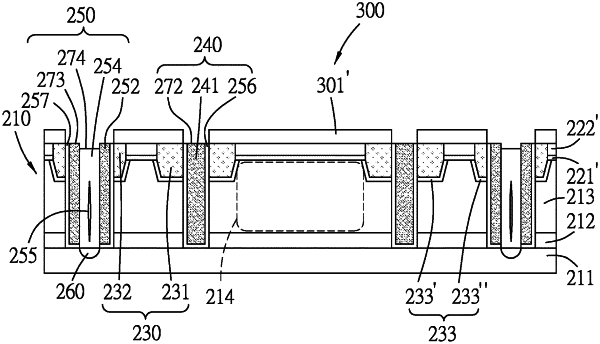
1. A semiconductor isolation structure comprising:
a silicon-on-insulator substrate including
a semiconductor substrate,
a buried insulation layer disposed on the semiconductor substrate, and
a semiconductor layer disposed on the buried insulation layer, and having a functional region;
a first deep trench isolation structure penetrating the semiconductor layer and the buried insulation layer, and surrounding the functional region;
a second deep trench isolation structure penetrating the semiconductor layer and the buried insulation layer, and surrounding the first deep trench isolation structure; and
a shallow trench isolation structure formed in the semiconductor layer and surrounding the functional region, the shallow trench isolation structure including a first shallow trench isolation that surrounds the functional region, and a second shallow trench isolation that surrounds the first shallow trench isolation, the first and second deep trench isolation structures respectively penetrating the first and second shallow trench isolations.
|