| CPC H01L 21/76254 (2013.01) [H01L 21/30604 (2013.01); H01L 21/84 (2013.01); H01L 21/02052 (2013.01)] | 17 Claims |
|
1. A method for preparing a silicon-on-insulator structure comprising a silicon top layer, a handle structure and dielectric layer disposed between the silicon top layer and handle structure, the method comprising:
implanting ions into a donor structure to form a cleave plane in the donor structure;
providing a handle structure;
forming a dielectric layer on at least one of the donor structure and handle structure prior to bonding;
bonding the donor structure to the handle structure to form a bonded wafer structure comprising the donor structure, handle structure and a dielectric layer disposed between the handle structure and the donor structure;
cleaving the bonded wafer structure at the cleave plane such that a portion of the donor structure remains bonded to the handle structure as a silicon top layer, the cleave forming a silicon-on-insulator structure comprising the handle structure, silicon top layer and dielectric layer disposed between the handle structure and silicon top layer;
annealing the silicon-on-insulator structure, an oxide forming on at least a top surface of the silicon-on-insulator structure during the anneal;
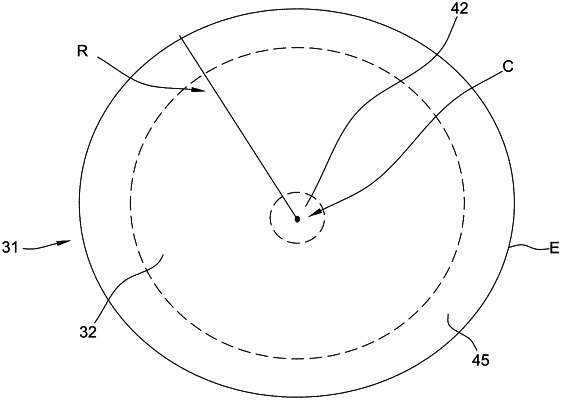
contacting a center region of the top surface of the silicon-on-insulator structure with an etching solution while spinning the silicon-on-insulator structure; and
contacting an edge region of the top surface of the silicon-on-insulator structure with the etching solution while spinning the silicon-on-insulator structure; and
depositing an epitaxial silicon layer on the silicon top layer after contacting the center region and the edge region of the top surface of the silicon-on-insulator structure.
|