| CPC H01L 21/31144 (2013.01) [H01L 21/76808 (2013.01); H01L 21/76877 (2013.01); H01L 23/528 (2013.01); H01L 23/5226 (2013.01)] | 20 Claims |
|
1. A semiconductor device comprising:
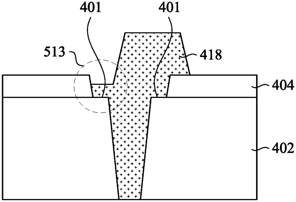
an insulating layer;
a via recess in the insulating layer;
a hard mask layer over an upper surface of the insulating layer and having an opening over the via recess such that portions of the upper surface of the insulating layer are exposed via the opening;
metal formed in the via recess, in the opening, and on the exposed upper surface of the insulating layer; and
a metal line over the via recess and in contact with the metal in the opening, wherein an axis of the metal line is offset from the center of the via recess.
|