| CPC H01G 4/30 (2013.01) [H01G 4/005 (2013.01); H01G 4/232 (2013.01); H01G 4/1218 (2013.01)] | 14 Claims |
|
1. A multilayer ceramic capacitor comprising:
a laminated body including a plurality of dielectric layers and a plurality of internal electrodes laminated in a lamination direction; and
a plurality of external electrodes electrically connected to respective ones of the internal electrodes; wherein
the laminated body includes a first principal surface and a second principal surface opposed in the lamination direction, a first side surface and a second side surface opposed in a width direction perpendicular or substantially perpendicular to the lamination direction, and a first end surface and a second end surface opposed in a length direction perpendicular or substantially perpendicular to both the lamination direction and the width direction;
the plurality of internal electrodes include first internal electrodes exposed at the first end surface, and second internal electrodes exposed at the second end surface;
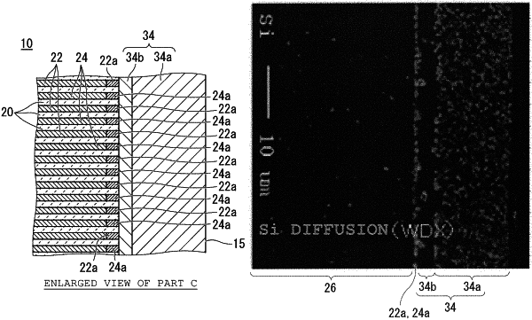
the laminated body includes outer layer portions provided at a top and a bottom of the laminated body in the lamination direction, and an inner layer portion between the outer layer portions;
the plurality of external electrodes include a first external electrode covering the first end surface and electrically connected to the first internal electrodes, and a second external electrode covering the second end surface and electrically connected to the second internal electrodes;
each of the first external electrode and the second external electrode includes a multilayer structure including a base electrode layer, a conductive resin layer on the base electrode layer, and a plating layer on the conductive resin layer;
side margin portions sandwich the plurality of dielectric layers in the width direction;
each of the side margin portions includes Si; and
in at least one cross sectional view in the width and lamination directions, the Si is included in a plurality of Si segregation portions in at least one of the side margin portions.
|