| CPC G11C 16/24 (2013.01) [G11C 7/12 (2013.01); G11C 11/005 (2013.01); G11C 16/0483 (2013.01); H10B 41/20 (2023.02); H10B 41/35 (2023.02)] | 20 Claims |
|
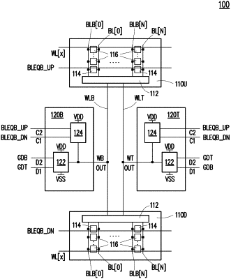
1. A write line circuit comprising:
a power supply node configured to carry a power supply voltage level;
a reference node configured to carry a reference voltage level;
a write line coupled to a plurality of bit lines of a memory array through a selection circuit;
an output node coupled to the write line;
first and second switching devices coupled in series between the output node and the power supply node, wherein a source of the first switching device is directly coupled exclusively to a drain of the second switching device;
an inverter comprising an output terminal coupled to a gate of the second switching device; and
a third switching device directly coupled to each of the output node and the reference node,
wherein
the first switching device is configured to selectively couple the output node to the second switching device responsive to a first data signal,
the second switching device and the inverter are configured to selectively couple the first switching device to the power supply node responsive to a second data signal, and
the third switching device is configured to selectively couple the output node to the reference node responsive to the first data signal.
|