US 11,798,603 B2
Circuit for generating and trimming phases for memory cell read operations
Vivek Tyagi, Ghaziabad (IN); Vikas Rana, Noida (IN); Chantal Auricchio, Cassina de'Pecchi (IT); and Laura Capecchi, Vedano al Lambro (IT)
Assigned to STMICROELECTRONICS S.r.l., Agrate Brianza (IT); and STMicroelectronics International N.V., Geneva (CH)
Filed by STMICROELECTRONICS S.r.l., Agrate Brianza (IT); and STMicroelectronics International N.V., Geneva (CH)
Filed on Feb. 27, 2023, as Appl. No. 18/175,375.
Application 18/175,375 is a continuation of application No. 17/542,203, filed on Dec. 3, 2021, granted, now 11,615,823.
Application 17/542,203 is a continuation of application No. 17/010,704, filed on Sep. 2, 2020, granted, now 11,205,462, issued on Dec. 21, 2021.
Claims priority of provisional application 62/899,005, filed on Sep. 11, 2019.
Prior Publication US 2023/0206971 A1, Jun. 29, 2023
Int. Cl. G11C 7/12 (2006.01); G11C 7/06 (2006.01); G11C 11/4094 (2006.01); G11C 11/4091 (2006.01); G11C 7/22 (2006.01)
CPC G11C 7/12 (2013.01) [G11C 7/065 (2013.01); G11C 7/222 (2013.01); G11C 11/4091 (2013.01); G11C 11/4094 (2013.01)] 20 Claims
OG exemplary drawing
 
1. A device, comprising:
an array of memory cells;
a plurality of bit lines coupled to the array of memory cells; and
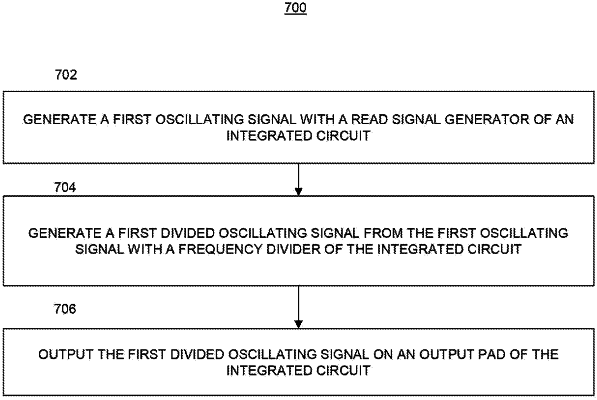
a read signal generator including:
a precharge signal generator including an input and an output and configured to generate a precharge signal including a precharge delay for timing precharging of the bitlines;
an evaluation signal generator including an input coupled to the output of the precharge signal generator and configured to generate an evaluation signal for evaluating data values stored in the memory cells during a read operation of the memory cells, the evaluation signal including an evaluation delay for timing evaluation of the data values; and
at least one switch configured to selectively cause the read signal generator to generate an oscillating signal to enable testing of at least one of the precharge delay and the evaluation delay.