| CPC G06V 40/1324 (2022.01) [G02B 3/0056 (2013.01)] | 10 Claims |
|
1. An electronic device comprising:
a substrate;
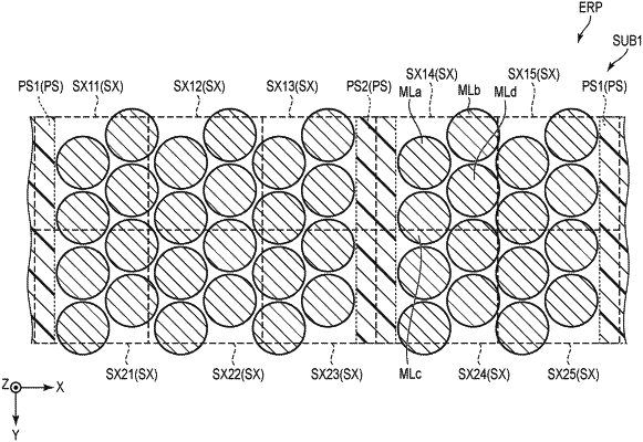
a plurality of sensor regions, each having a plurality of sensor elements on the substrate;
a plurality of microlenses arranged in a hexagonal periodic structure over the plurality of sensor elements in a first direction and a second direction that intersect each other, and provided in the plurality of sensor regions; and
a plurality of spacers arranged on the substrate and between the plurality of sensor regions, wherein
the plurality of sensor regions include a first sensor region adjacent to the plurality of spacers, a second sensor region adjacent to the first sensor region in the first direction, and a third sensor region adjacent to the first sensor region in the second direction, and include at least one microlens overlapped with the first sensor region and the second sensor region, and at least one microlens overlapped with the first sensor region and the third sensor region,
the plurality of spacers include a first spacer, a second spacer, and a third spacer, and
the number of rows of the sensor regions between the first spacer and the second spacer, and the number of rows of the sensor regions between the second spacer and the third spacer are different.
|