US 11,797,834 B2
Compensation for reference transistors and memory cells in analog neuro memory in deep learning artificial neural network
Hieu Van Tran, San Jose, CA (US); Vipin Tiwari, Dublin, CA (US); and Nhan Do, Saratoga, CA (US)
Assigned to SILICON STORAGE TECHNOLOGY, INC., San Jose, CA (US)
Filed by Silicon Storage Technology, Inc., San Jose, CA (US)
Filed on Aug. 10, 2022, as Appl. No. 17/885,431.
Application 17/885,431 is a division of application No. 16/150,606, filed on Oct. 3, 2018, granted, now 11,443,175.
Claims priority of provisional application 62/696,718, filed on Jul. 11, 2018.
Prior Publication US 2022/0391682 A1, Dec. 8, 2022
Int. Cl. G06N 3/065 (2023.01); G11C 11/56 (2006.01); G06F 3/06 (2006.01); G06F 17/16 (2006.01); G06N 3/08 (2023.01); G11C 13/00 (2006.01); G11C 16/04 (2006.01); G11C 16/28 (2006.01); G06N 3/048 (2023.01)
CPC G06N 3/065 (2023.01) [G06F 3/061 (2013.01); G06F 3/0688 (2013.01); G06F 17/16 (2013.01); G06N 3/048 (2023.01); G06N 3/08 (2013.01); G11C 11/5642 (2013.01); G11C 13/004 (2013.01); G11C 16/0425 (2013.01); G11C 16/28 (2013.01); G11C 2211/563 (2013.01); G11C 2213/15 (2013.01)] 16 Claims
OG exemplary drawing
 
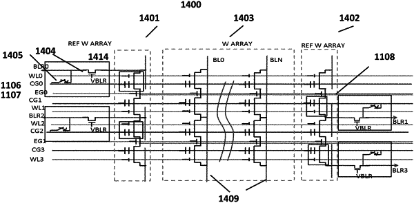
1. A method comprising:
receiving a first voltage;
multiplying the first voltage by a coefficient to generate a second voltage;
applying the first voltage to one of a gate of a reference transistor and a gate of a selected memory cell;
applying the second voltage to the other of the gate of the reference transistor and the gate of the selected memory cell; and
using the reference transistor in a sense operation to determine a value stored in the selected memory cell.