| CPC G06F 30/398 (2020.01) [G06F 2117/04 (2020.01)] | 20 Claims |
|
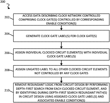
1. A non-transitory computer-readable medium comprising instructions that, when executed by a hardware processor of a device, cause the device to perform operations comprising:
accessing data that describes a clock network of a circuit design, the clock network comprising a set of clock gates controlled by a corresponding set of enable conditions, the set of clock gates controlling clock signals to a set of clocked circuit elements of the circuit design;
generating a set of clock gate labels for the set of clock gates by, for each individual clock gate in the set of clock gates:
assigning a clock gate label to the individual clock gate; and
associating the clock gate label with an individual enable condition, from the corresponding set of enable conditions, for the individual clock gate;
for each individual clocked circuit element in the set of clocked circuit elements, assigning a select label from the set of clock gate labels to the individual clocked circuit element, the select label corresponding to a select clock gate that controls a clock signal to the individual clocked circuit element;
assigning an ungated label to all other clocked circuit elements that are not controlled by any clock gates; and
removing redundant logic from the circuit design by performing a depth-first search of the circuit design starting from each clocked circuit element of the circuit design.
|