| CPC G06F 30/392 (2020.01) [H01L 27/0207 (2013.01); G06F 2119/18 (2020.01)] | 20 Claims |
|
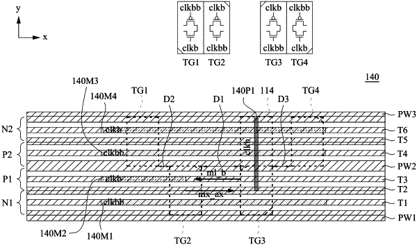
1. A semiconductor device, comprising:
a first conductive pattern disposed within a first row from a top view perspective and extending along a first direction;
a first phase shift circuit disposed within the first row;
a first transmission circuit disposed within a second row from the top view perspective; and
a first gate conductor extending from the first row to the second row along a second direction perpendicular to the first direction, wherein
each of the first and second rows comprises first and second active regions extending along the first direction, and
the first phase shift circuit and the first transmission circuit are electrically connected with the first conductive pattern through the first gate conductor.
|