| CPC G06F 3/147 (2013.01) [G06F 3/1423 (2013.01); H04N 23/815 (2023.01); H04N 25/76 (2023.01)] | 24 Claims |
|
1. A device comprising:
an imaging unit including a plurality of photoelectric conversion elements;
a processing unit configured to process a signal transmitted from the imaging unit and having an artificial intelligence (AI) unit; and
a display unit configured to display an image based on the signal processed by the processing unit,
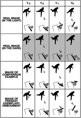
wherein the processing unit is configured to process first image information at a first time from the imaging unit, and configured to generate first prediction image information with respect to a second time later than the first time based on the first image information,
wherein the imaging unit includes a first semiconductor substrate having the plurality of photoelectric conversion elements and a second semiconductor substrate having one or more circuits for processing signals from the plurality of photoelectric conversion elements, and
wherein the first semiconductor substrate and the second semiconductor substrate are laminated.
|