| CPC G03G 15/5062 (2013.01) [H04N 1/32138 (2013.01)] | 20 Claims |
|
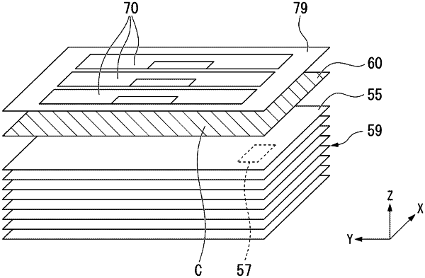
1. A conductive sheet that is configured to be positioned between a sheet tray of an image forming device and a sheet, the conductive sheet comprising:
a base layer comprising a conductive material positioned to overlap with a wireless tag of the sheet; and
a double conveyance prevention structure coupled to or defined by the base layer, the double conveyance prevention structure configured to prevent conveyance of the conductive sheet by the image forming device when the conductive sheet overlaps the sheet in the sheet tray.
|