| CPC G02F 1/1368 (2013.01) [G02F 1/136209 (2013.01); G02F 1/136227 (2013.01)] | 16 Claims |
|
1. An array substrate, comprising:
a base substrate;
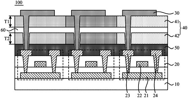
a thin-film transistor disposed on a side of the base substrate, wherein the thin-film transistor comprises at least a first electrode;
a pixel electrode disposed on a side of the thin-film transistor facing away from the base substrate; and
at least two color resist layers disposed between the thin-film transistor and the pixel electrode, wherein a medium layer is disposed between any two adjacent color resist layers of the at least two color resist layers,
wherein the pixel electrode is electrically connected to the first electrode of the thin-film transistor through a via, and the via penetrates through the at least two color resist layers and the medium layer disposed between the any two adjacent color resist layers,
wherein the array substrate further comprises a planarization layer disposed between the pixel electrode and the thin-film transistor, and the planarization layer is an insulating layer,
wherein the at least two color resist layers are disposed between the planarization layer and the pixel electrode; or, the at least two color resist layers are disposed between the planarization layer and the thin-film transistor; or the at least two color resist layers comprise at least one first color resist layer and at least one second color resist layer, wherein the at least one first color resist layer is disposed between the planarization layer and the pixel electrode, and the at least one second color resist layer is disposed between the planarization layer and the thin-film transistor.
|