| CPC G02B 6/12002 (2013.01) [G02B 6/12004 (2013.01); G02B 6/136 (2013.01)] | 20 Claims |
|
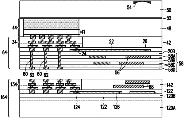
1. A method comprising:
forming a first photonic die comprising:
forming a first silicon waveguide; and
forming a first nitride waveguide;
forming a first through-via extending into a first plurality of dielectric layers in the first photonic die;
bonding a second photonic die to the first photonic die, wherein the second photonic die comprises:
a second nitride waveguide, wherein the first silicon waveguide is optically coupled to the second nitride waveguide through the first nitride waveguide;
forming a second through-via extending into a second plurality of dielectric layers in the second photonic die; and
bonding an electronic die to the first photonic die, wherein the second through-via is electrically coupled to the electronic die through the first through-via, and wherein the electronic die comprises circuits for processing electrical signals from the first photonic die.
|