| CPC F21V 9/40 (2018.02) [F21V 7/26 (2018.02); F21V 29/502 (2015.01); F21V 29/70 (2015.01)] | 20 Claims |
|
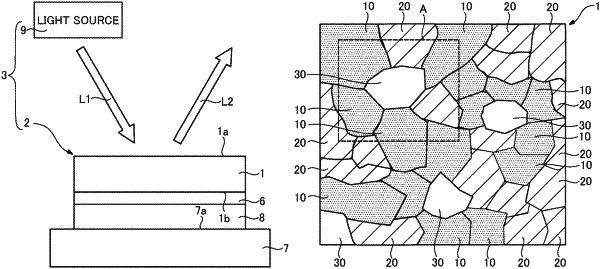
1. A fluorescent plate comprising:
a fluorescent phase which emits fluorescence by excitation light,
a light-transmitting phase which allows passage of the excitation light, and
a plurality of voids surrounded by the fluorescent phase and the light-transmitting phase,
wherein, in a cross section of the fluorescent plate including cross sections of the voids, an average ratio of a portion of the circumference of a void, which portion is in contact with the fluorescent phase to the entire circumference of the void, is higher than
a ratio of the area of the fluorescent phase present in the fluorescent plate to the total area of the fluorescent phase and the light-transmitting phase present in the fluorescent plate.
|