| CPC C30B 29/36 (2013.01) [C23C 16/325 (2013.01); C23C 16/4408 (2013.01); C23C 16/52 (2013.01); C30B 25/16 (2013.01); C30B 25/205 (2013.01); H01L 21/0262 (2013.01); H01L 21/02378 (2013.01); H01L 21/02532 (2013.01); H01L 21/02579 (2013.01); H01L 29/167 (2013.01); H01L 29/1608 (2013.01)] | 7 Claims |
|
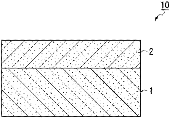
1. A SiC epitaxial wafer, comprising:
a SiC substrate; and,
an epitaxial layer of SiC laminated on the SiC substrate,
wherein the epitaxial layer contains an impurity element which determines the conductivity type of the epitaxial layer and boron which has a conductivity type different from the conductivity type of the impurity element, and
the concentration of boron is less than 1.0×1014 cm−3 at any position in the plane of the epitaxial layer.
|