| CPC H10N 60/805 (2023.02) [G06N 10/00 (2019.01); H01P 3/003 (2013.01); H01P 5/022 (2013.01); H01P 5/028 (2013.01); H01P 11/001 (2013.01); H10N 60/0912 (2023.02); H10N 60/12 (2023.02); H10N 60/85 (2023.02)] | 16 Claims |

|
1. A method of fabricating a device, comprising:
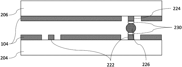
providing a first substrate with a principal surface, wherein the first substrate comprises a first portion of a circuit element having a microwave frequency resonance mode;
providing a second substrate with a principal surface, wherein the second substrate comprises a second portion of the circuit element having the microwave frequency resonance mode; and
bonding the first substrate to the second substrate with a plurality of bump bonds, wherein a first bump bond of the plurality of bump bonds connects the first portion of the circuit element to the second portion of the circuit element to provide an electrical connection between the first portion and the second portion, wherein the circuit element is a qubit.
|