| CPC H10K 77/111 (2023.02) [H10K 59/1213 (2023.02); H10K 59/131 (2023.02); H10K 71/00 (2023.02); H10K 71/80 (2023.02); H01L 27/1218 (2013.01); H01L 27/1225 (2013.01); H01L 27/124 (2013.01); H01L 27/1251 (2013.01); H01L 27/1266 (2013.01); H01L 27/127 (2013.01); H01L 27/1288 (2013.01); H01L 29/66757 (2013.01); H01L 29/66969 (2013.01); H01L 29/78675 (2013.01); H01L 29/7869 (2013.01); H10K 59/1201 (2023.02); H10K 2102/311 (2023.02)] | 14 Claims |

|
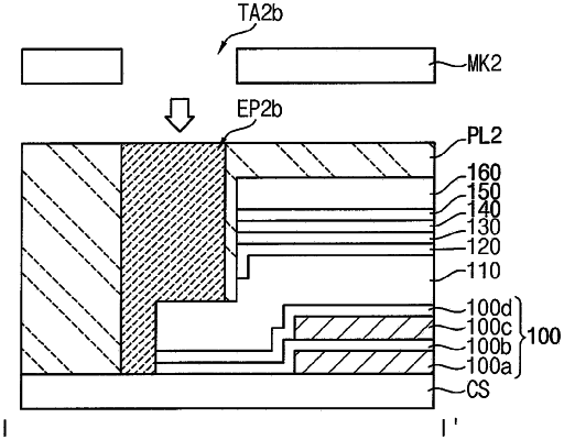
1. A method for manufacturing a display device, the method comprising:
forming a base substrate on a carrier substrate, the base substrate including:
an organic film including a polymeric material; and
an inorganic barrier film overlapping the organic film and extending outwardly from an edge of the organic film;
forming a first active pattern including a semiconductive material in a display area of the base substrate;
forming a first interlayer insulation layer on the first active pattern;
forming a second active pattern on the first interlayer insulation layer in the display area of the base substrate, the second active pattern including a semiconductive material different from the first active pattern;
forming a second interlayer insulation layer on the second active pattern;
forming a photoresist film on the second interlayer insulation layer;
exposing the photoresist film to light through a first mask including:
a first transmitting portion overlapping the first active pattern or the second active pattern; and
a second transmitting portion disposed between an edge of the carrier substrate and the edge of the organic film;
exposing an edge portion of the photoresist film to light, the edge portion of the photoresist film overlapping the edge of the carrier substrate;
developing the photoresist film to form a first photoresist pattern that includes a first opening and does not overlap the edge of the carrier substrate, the first opening overlapping the first active pattern or the second active pattern; and
forming a contact hole exposing the first active pattern or the second active pattern by using the first photoresist pattern as a mask.
|