| CPC H10K 59/131 (2023.02) [G09G 3/3258 (2013.01); H01L 27/124 (2013.01); H10K 59/1213 (2023.02); H10K 59/1216 (2023.02); G09G 2300/0426 (2013.01)] | 20 Claims |

|
1. A display apparatus comprising:
a substrate having a display area and a non-display area outside the display area, the display area being an area in which light is emitted;
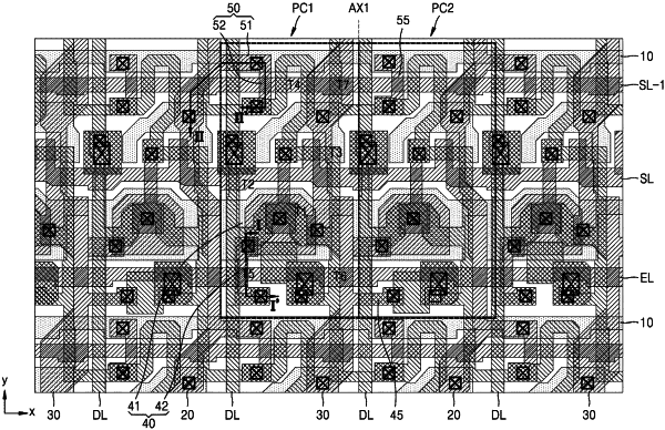
a first pixel circuit in the display area and including a first driving thin-film transistor and a first storage capacitor electrically connected to the first driving thin-film transistor;
a second pixel circuit adjacent to the first pixel circuit and including a second driving thin-film transistor and a second storage capacitor electrically connected to the second driving thin-film transistor;
a first initialization voltage line electrically connected to the first pixel circuit and the second pixel circuit and extending in a first direction;
a second initialization voltage line electrically connected to the first initialization voltage line and extending in a second direction crossing the first direction and crossing over the first initialization voltage line in the display area to form a mesh structure, the mesh structure overlapping the area in which light is emitted when viewed in a plan view; and
a driving voltage line extending in the second direction between the first pixel circuit and the second pixel circuit,
wherein a channel area of the first driving thin-film transistor in the first pixel circuit in the display area of the substrate or a channel area of the second driving thin-film transistor in the second pixel circuit in the display area of the substrate is between the second initialization voltage line and the driving voltage line when viewing the substrate in the plan view.
|