| CPC H10K 59/126 (2023.02) [G09G 3/3266 (2013.01); G09G 3/3291 (2013.01); H10K 59/1213 (2023.02); H10K 59/1216 (2023.02); H10K 59/131 (2023.02); G09G 2320/045 (2013.01)] | 10 Claims |

|
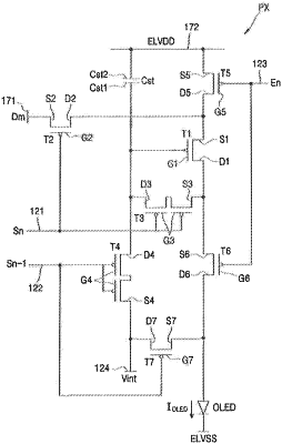
1. A display device comprising:
a first transistor comprising a first semiconductor layer and a first gate electrode on the first semiconductor layer;
a storage capacitor overlapping the first semiconductor layer and comprising a first electrode and a second electrode on the first electrode;
a data line extending in a first direction;
a second transistor electrically coupled to the data line, the second transistor comprising a second semiconductor layer and a second gate electrode on the second semiconductor layer;
a third transistor electrically coupled to the first transistor, the third transistor comprising a third semiconductor layer and a third gate electrode on the third semiconductor layer;
a light emitting diode including a pixel electrode, an opposite electrode, and an emission layer between the pixel electrode and the opposite electrode; and
a driving voltage line extending in the first direction, wherein the driving voltage line comprises:
an extending part extending in the first direction; and
a protrusion part protruding from the extending part along a second direction crossing the first direction, and
wherein the driving voltage line overlaps the third transistor and the pixel electrode and extends continuously from the third transistor to overlap the storage capacitor and the first transistor.
|