| CPC H10K 59/124 (2023.02) [H10K 71/00 (2023.02); H10K 50/15 (2023.02); H10K 50/16 (2023.02); H10K 50/17 (2023.02); H10K 50/171 (2023.02); H10K 50/844 (2023.02); H10K 59/12 (2023.02); H10K 59/1201 (2023.02); H10K 59/122 (2023.02); H10K 59/131 (2023.02); H10K 59/35 (2023.02); H10K 59/352 (2023.02); H10K 77/111 (2023.02); H10K 2102/311 (2023.02)] | 13 Claims |

|
1. A display device comprising:
a substrate having flexibility and made of resin,
a thin film transistor (TFT) layer provided on the substrate,
a light-emitting element layer provided on the TFT layer,
a display region configured to display an image through light emission in the light-emitting element layer, and a frame region is located around the display region,
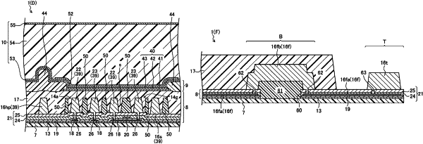
the TFT layer including an inorganic insulating film, a conductive portion provided on the inorganic insulating film, and a flattening film covering the conductive portion,
the light-emitting element layer including a first electrode provided on the flattening film, a light emission function layer provided on the first electrode, and a second electrode overlapping the first electrode with the light emission function layer interposed between the second electrode and the first electrode,
a terminal section provided at an end portion of the frame region,
a bending portion provided in the frame region located between the display region and the terminal section,
a slit formed in the inorganic insulating film, a frame flattening film filling the slit,
a plurality of the conductive portions provided below the first electrode and conductive portions of the plurality of conductive portions adjacent to each other at intervals, and
a flattening auxiliary film provided between every adjacent conductive portions of the plurality of conductive portions, the flattening auxiliary film formed of a material identical to a material of the frame flattening film in a layer identical to a layer of the frame flattening film, the flattening auxiliary film and the conductive portions covered by the flattening film.
|