| CPC H10K 59/1213 (2023.02) [H10K 59/131 (2023.02)] | 10 Claims |

|
1. A display device comprising a first layer and a second layer over the first layer,
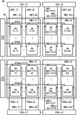
wherein the first layer comprises first circuits arranged in m rows and n columns (m and n are each an integer greater than or equal to 1 and a product of m and n is an integer greater than or equal to 2),
wherein the second layer comprises pixel blocks arranged in the m rows and the n columns,
wherein the pixel blocks each comprise pixels arranged in a rows and b columns (a and b are each an integer greater than or equal to 1),
wherein the pixel block comprises a first wiring and a second wiring electrically connected to the pixel,
wherein the first wiring and the second wiring included in the pixel block in an i-th row and a j-th column (i is an integer greater than or equal to 1 and less than or equal to m, and j is an integer greater than or equal to 1 and less than or equal to n) are each electrically connected to the first circuit in the i-th row and the j-th column,
wherein the first wiring is configured to supply an input signal from the first circuit to the pixel,
wherein the second wiring is configured to supply an output signal from the pixel to the first circuit,
wherein each of the first circuits comprises a correction data generation circuit, a logic circuit, and a source driver circuit,
wherein the correction data generation circuit is configured to convert the output signal into correction data,
wherein the logic circuit is configured to correct a video signal input to the first circuit on the basis of the correction data and generating the corrected video signal, and
wherein the source driver circuit is configured to convert the corrected video signal into the input signal.
|