| CPC H10B 43/40 (2023.02) [H10B 41/10 (2023.02); H10B 41/27 (2023.02); H10B 41/35 (2023.02); H10B 41/40 (2023.02); H10B 43/10 (2023.02); H10B 43/27 (2023.02); H10B 43/35 (2023.02)] | 17 Claims |

|
1. A semiconductor device, comprising:
a lower structure including a peripheral circuit and peripheral pads electrically connected to the peripheral circuit;
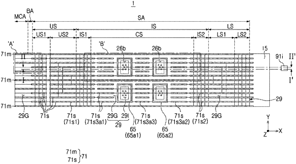
a stack structure on the lower structure, extending from a memory cell array region through a stepped region adjacent to the memory cell array region, and including a gate stacked region that includes gate stack materials, and insulator stacked regions on the stepped region of the stack structure;
a capping insulating structure on the stack structure;
vertical memory structures passing through the gate stacked region of the stack structure in the memory cell array region;
separation structures passing through the gate stacked region of the stack structure and extending into the capping insulating structure; and
peripheral contact structures passing through at least one of the insulator stacked regions, and extending into the capping insulating structure, wherein:
the stack structure includes interlayer insulating layers and horizontal layers, alternately and repeatedly stacked in the memory cell array region, and extending from the memory cell array region into the stepped region,
the horizontal layers include gate horizontal layers and insulating horizontal layers, the gate horizontal layers being included in the gate stacked region, and each of the insulator stacked regions including the insulating horizontal layers,
in the stepped region, the stack structure includes a first stepped region farther from the lower structure than a second stepped region, and a connection stepped region between the first stepped region and the second stepped region, arranged in different height levels above the lower structure and extending away in a first direction from the memory cell array region,
the insulator stacked regions are spaced apart in the connection stepped region in the first direction,
the separation structures include a pair of main separation structures parallel to each other, and a plurality of dummy separation structures between the pair of main separation structures, the pair of main separation structures extending through the memory cell array region, a buffer region, the stepped region, and into the capping insulating structure of the stack structure;
the insulator stacked regions are disposed between the pair of main separation structures, and
the plurality of dummy separation structures pass through the connection stepped region of the stack structure, and are spaced apart from the insulator stacked regions.
|