| CPC H10B 12/30 (2023.02) [H01L 21/6835 (2013.01); H01L 29/0673 (2013.01); H01L 29/42392 (2013.01); H01L 29/66742 (2013.01); H01L 29/78618 (2013.01); H01L 29/78696 (2013.01); H10B 12/03 (2023.02); H10B 12/05 (2023.02); H10B 53/30 (2023.02); H01L 2221/68363 (2013.01)] | 20 Claims |

|
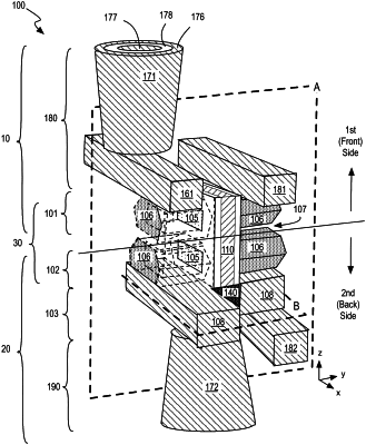
1. An integrated circuit (IC) comprising: an array of memory cells, wherein individual ones of the memory cells comprise:
a stacked field effect transistor structure, comprising:
a stack of channel regions comprising a semiconductor material;
one or more gate electrodes around the stack of channel regions; and
a stack of source and drain regions comprising a first pair of source and drain regions electrically coupled to a first of the channel regions, and over a second pair of source and drain regions electrically coupled to a second of the channel regions;
a first capacitor comprising a metal-insulator-metal (MIM) structure on a first side of the stacked transistor structure, wherein the first capacitor comprises a first terminal that is electrically coupled to a first of the first pair of source and drain regions; and
a second capacitor comprising a MIM structure on a second side of the stacked transistor structure, opposite the first side, wherein the second capacitor comprises a terminal that is electrically coupled to a first of the second pair of source and drain regions; and
cell addressing interconnects coupled to each of the memory cells, wherein the cell addressing interconnects comprise:
an interconnect on the first side of the stacked transistor structure and electrically coupled to a terminal of the stacked transistor structure in two or more of the memory cells; and
an interconnect on the second side of the stacked transistor structure and electrically coupled to a terminal of the stacked transistor structure or of the second capacitor in two or more of the memory cells.
|