|
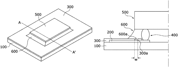
1. A printed circuit board comprising: a base board; a metal layer including a pad and a metal line formed on the base board; a solder resist layer formed on the base board on which the metal layer is formed and formed with an opening through which a surface of the metal line is exposed; and an underfill formed between the solder resist layer and a semiconductor chip electrically connected to the pad, and including a blocking area formed in the opening, wherein the blocking area is formed to surround a portion of the semiconductor chip along an edge of the semiconductor chip, and wherein the blocking area is formed in an area where the metal line is formed among the entire edge of the semiconductor chip.
|
