| CPC H05K 1/024 (2013.01) [H05K 1/0231 (2013.01); H05K 1/0243 (2013.01); H05K 3/4673 (2013.01); H05K 3/4688 (2013.01); H05K 1/0306 (2013.01); H05K 1/036 (2013.01); H05K 1/0366 (2013.01); H05K 2201/0187 (2013.01)] | 23 Claims |

|
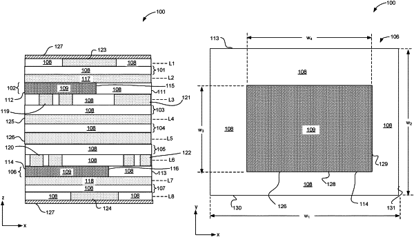
1. A printed circuit board (PCB), comprising:
a first layer comprising a first dielectric material substantially exclusively; and
a second layer comprising the first dielectric material within a first region and a second dielectric material within a second region adjacent to the first region, wherein:
the first dielectric material has a first dielectric constant, a first coefficient of thermal expansion (CTE) and a first glass transition temperature (Tg);
the second dielectric material has a second dielectric constant, a second CTE and a second Tg;
the first dielectric constant is a greater than the second dielectric constant;
the first CTE is substantially equal to the second CTE; and
the first Tg and the second Tg are greater than 150° C.
|