| CPC H04N 25/778 (2023.01) [H04N 25/60 (2023.01); H04N 25/772 (2023.01)] | 13 Claims |
|
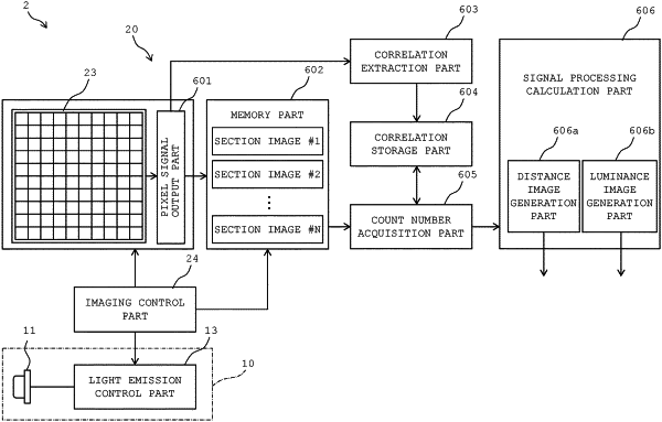
9. An imaging device comprising:
a solid-state imaging element having a plurality of pixel cells arranged in a matrix; and
a signal processing part configured to process a detection signal outputted from each of the pixel cells, wherein
the pixel cells each include an avalanche photodiode,
during an exposure period of the pixel cells, the pixel cells accumulate charges from the avalanche photodiode to output a voltage corresponding to the accumulated charges as the detection signal, wherein the accumulated charges correspond to a count number of photons received by the avalanche photodiode during the exposure period, and
the signal processing part includes
a correlation extraction part configured to extract a correlation between the count number and the detection signal for each of the pixel cells, and
a count number acquisition part configured to acquire the count number corresponding to the detection signal from each of the pixel cells on the basis of the correlation extracted by the correlation extraction part.
|