| CPC H03K 3/017 (2013.01) [H03K 5/01 (2013.01); H03L 7/0812 (2013.01); H03K 2005/00019 (2013.01)] | 17 Claims |

|
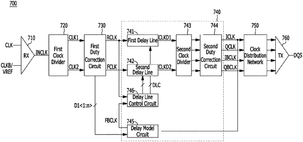
1. A semiconductor apparatus comprising:
a clock divider configured to generate a first divided clock signal and a second divided clock signal by dividing an input clock signal;
a first duty correction circuit configured to generate a first reference clock signal and a second reference clock signal by delaying the first and second divided clock signals, compare the phases of the first and second reference clock signals to adjust a delay time of the second divided clock signal by a first time, and then decrease a delay time of the first divided clock signal and the delay time of the second divided clock signal by a second time; and
a delay locked loop circuit configured to compare the phases of the first reference clock signal and a feedback clock signal and generate at least one output clock signal by delaying the first and second reference clock signals, and generate the feedback clock signal by delaying the at least one output clock signal.
|