| CPC H01S 5/2202 (2013.01) [H01S 5/2214 (2013.01); H01S 5/34333 (2013.01); H01L 21/0254 (2013.01); H01L 21/02576 (2013.01); H01L 21/02579 (2013.01); H01L 21/02581 (2013.01); H01S 5/04253 (2019.08); H01S 5/04257 (2019.08); H01S 5/2009 (2013.01); H01S 5/2031 (2013.01); H01S 5/305 (2013.01); H01S 5/3063 (2013.01); H01S 5/3213 (2013.01); H01S 2301/176 (2013.01); H01S 2304/00 (2013.01)] | 22 Claims |

|
1. A manufacturing method of a nitride-based semiconductor light-emitting element, the manufacturing method comprising:
forming an n-type nitride-based semiconductor layer;
forming, on the n-type nitride-based semiconductor layer, a light emission layer including a nitride-based semiconductor;
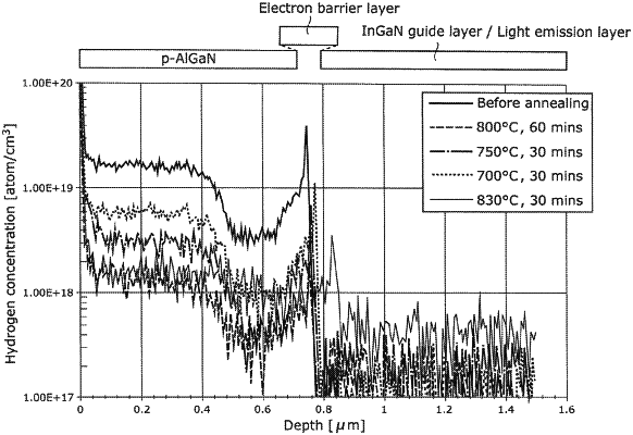
forming, on the light emission layer in an atmosphere containing a hydrogen gas, a p-type nitride-based semiconductor layer while doping the p-type nitride-based semiconductor layer with a p-type dopant at a concentration of at least 2.0×10¹⁸ atom/cm3; and
annealing the p-type nitride-based semiconductor layer at a temperature of at least 800 degrees Celsius in an atmosphere not containing hydrogen,
wherein a hydrogen concentration of the p-type nitride-based semiconductor layer after the annealing is at most 5.0×10¹⁸ atom/cm3 and at most 5% of the concentration of the p-type dopant, and
a hydrogen concentration of the light emission layer is at most 2.0×10¹⁷ atom/cm3.
|