| CPC H01S 5/18361 (2013.01) [H01S 5/04254 (2019.08); H01S 5/18311 (2013.01); H01S 5/34333 (2013.01); H01S 5/34346 (2013.01)] | 12 Claims |

|
1. A light emitting element comprising:
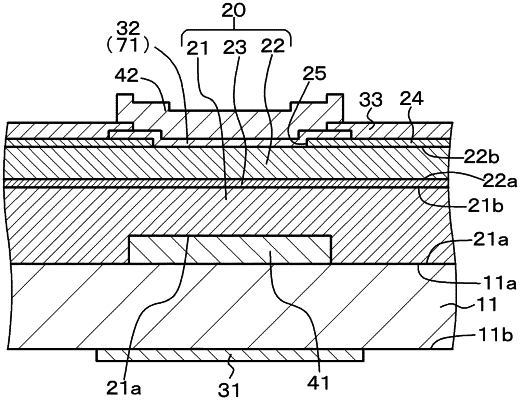
a stacked structure including, in a stacked state,
a first light reflection layer in which a plurality of thin films is stacked,
a light emitting structure, and
a second light reflection layer in which a plurality of thin films is stacked,
wherein the light emitting structure includes
a first compound semiconductor layer,
an active layer, and
a second compound semiconductor layer, that are stacked from a first light reflection layer side,
the light emitting structure is formed with a light absorbing material layer in parallel to a virtual plane occupied by the active layer, and
where a wavelength of light which is emitted from the active layer and which has a maximum intensity be λ0, an equivalent refractive index of layers occupying layers ranging from the active layer to the light absorbing material layer is neq, an optical distance from the active layer to the light absorbing material layer is Lop, and let λ≡{(2m+1)λ0}/(4neq) (where m is an integer of equal to or more than 0), then,
a value of Lop is a value different from A, and
a thickness Tave of a light reflection layer on a side on which the light absorbing material layer is located is a value different from a thickness TDBR, and
where refractive indexes of thin films constituting the light reflection layer on the side on which the light absorbing material layer is located is ni and the total number of the thin films is 1, then,
TDBR=Σ(Λ0/4ni),
i=1, 2, 3, . . . , 1, and
“Σ” means to sum up from i=1 to i=1,
wherein the first compound semiconductor layer, the active layer, and the second compound semiconductor layer include a GaN-based compound semiconductor material.
|