| CPC H01P 3/121 (2013.01) [H01P 5/082 (2013.01); H01P 5/107 (2013.01); H01P 11/002 (2013.01); H01Q 1/2283 (2013.01)] | 19 Claims |

|
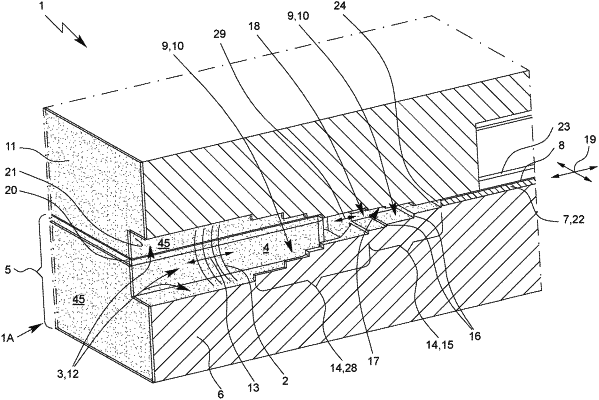
1. A method for manufacturing a waveguide arrangement comprising a cavity surrounded by conductive material for guiding electromagnetic waves,
wherein at least part of the cavity is produced by removing from a printed circuit board material for manufacturing printed circuits, having at least one plate-shaped back and a conductive layer, in sections the conductive layer and parts of the back, whereby a surface structure in the form of a recess is formed, and wherein an electrically conductive wall is subsequently formed by depositing conductive material, which wall delimits the cavity.
|