| CPC H01L 33/60 (2013.01) [H01L 33/486 (2013.01); H01L 33/507 (2013.01); H01L 33/56 (2013.01); H01L 33/62 (2013.01); H01L 2933/0041 (2013.01); H01L 2933/005 (2013.01); H01L 2933/0058 (2013.01); H01L 2933/0066 (2013.01)] | 18 Claims |

|
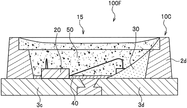
1. A light emitting device comprising:
a package in which a recess is defined;
a light emitting element and a protection device respectively disposed on a bottom surface defining the recess;
a first reflecting layer covering a lateral surface defining the recess; and
a second reflecting layer covering the bottom surface defining the recess, wherein:
the first reflecting layer is apart from the light emitting element and covers the protection device,
the second reflecting layer contacts a lower portion of a lateral surface of the light emitting element, and
an upper surface of the light emitting element and an upper portion of the lateral surface of the light emitting element are exposed from the second reflecting layer.
|