US 12,119,416 B2
Buffer layers for photovoltaic devices with group V doping
Le Chen, Fremont, CA (US); Sachit Grover, Campbell, CA (US); Jason Kephart, San Jose, CA (US); Sergei Kniajanski, Clifton Park, NY (US); Chungho Lee, San Jose, CA (US); Xiaoping Li, Santa Clara, CA (US); Feng Liao, Perrysburg, OH (US); Dingyuan Lu, San Jose, CA (US); Rajni Mallick, Fremont, CA (US); Wenming Wang, Toledo, OH (US); Gang Xiong, Santa Clara, CA (US); and Wei Zhang, San Jose, CA (US)
Assigned to First Solar, Inc., Tempe, AZ (US)
Appl. No. 17/287,988
Filed by First Solar, Inc., Tempe, AZ (US)
PCT Filed Oct. 23, 2019, PCT No. PCT/US2019/057542
§ 371(c)(1), (2) Date Apr. 22, 2021,
PCT Pub. No. WO2020/086646, PCT Pub. Date Apr. 30, 2020.
Claims priority of provisional application 62/866,665, filed on Jun. 26, 2019.
Claims priority of provisional application 62/834,017, filed on Apr. 15, 2019.
Claims priority of provisional application 62/833,312, filed on Apr. 12, 2019.
Claims priority of provisional application 62/749,934, filed on Oct. 24, 2018.
Prior Publication US 2021/0376177 A1, Dec. 2, 2021
Int. Cl. H01L 31/0216 (2014.01); H01L 31/0296 (2006.01); H01L 31/073 (2012.01)
CPC H01L 31/02167 (2013.01) [H01L 31/02963 (2013.01); H01L 31/073 (2013.01)] 24 Claims
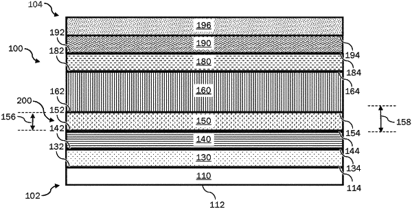
OG exemplary drawing
 
1. A photovoltaic device comprising:
a substrate;
a transparent conductive oxide layer over the substrate;
a buffer layer residing over the transparent conductive oxide layer, the buffer layer including:
a first buffer layer comprising a discontinuous first layer including MnOx and a void formed through the discontinuous first layer occupied by a material other than MnOx; and
a second buffer layer;
an absorber layer over the buffer layer, the absorber layer including a group V dopant, and the absorber layer having a first and second surface; and
a back contact layer over the absorber layer.