| CPC H01L 29/872 (2013.01) [H01L 29/0623 (2013.01); H01L 29/402 (2013.01)] | 10 Claims |

|
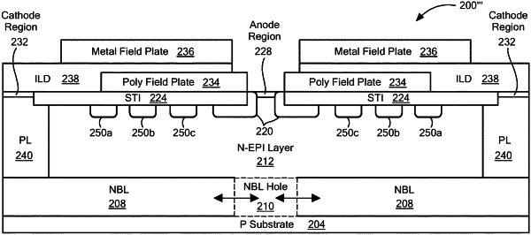
1. A Schottky diode comprising:
a substrate having a first type dopant;
a buried layer within the substrate and having a second type dopant;
an epitaxial layer above the buried layer and having the second type dopant;
a plurality of rings within the epitaxial layer and having the first type dopant, wherein the plurality of rings comprises an L-shaped ring;
a shallow trench isolation (STI) layer at the top region of the epitaxial layer;
an anode;
a cathode spaced from the anode by the STI layer; and
wherein the buried layer has an open region substantially vertically aligned with the anode.
|