US 12,119,409 B2
Multi-layer crystalline back gated thin film transistor
Van H. Le, Portland, OR (US); Abhishek A. Sharma, Hillsboro, OR (US); Gilbert Dewey, Hillsboro, OR (US); Kent Millard, Hillsboro, OR (US); Jack Kavalieros, Portland, OR (US); Shriram Shivaraman, Hillsboro, OR (US); Tristan A. Tronic, Aloha, OR (US); Sanaz Gardner, Portland, OR (US); Justin R. Weber, Hillsboro, OR (US); Tahir Ghani, Portland, OR (US); Li Huey Tan, Hillsboro, OR (US); and Kevin Lin, Beaverton, OR (US)
Assigned to Intel Corporation, Santa Clara, CA (US)
Filed by Intel Corporation, Santa Clara, CA (US)
Filed on Jun. 30, 2023, as Appl. No. 18/345,641.
Application 18/345,641 is a continuation of application No. 17/472,879, filed on Sep. 13, 2021, granted, now 11,764,306.
Application 17/472,879 is a continuation of application No. 16/640,340, granted, now 11,152,514, issued on Oct. 19, 2021, previously published as PCT/US2017/054589, filed on Sep. 29, 2017.
Prior Publication US 2023/0352598 A1, Nov. 2, 2023
This patent is subject to a terminal disclaimer.
Int. Cl. H01L 29/786 (2006.01); H01L 27/12 (2006.01); H01L 29/66 (2006.01); H01L 29/267 (2006.01)
CPC H01L 29/78693 (2013.01) [H01L 27/1207 (2013.01); H01L 27/1225 (2013.01); H01L 27/1255 (2013.01); H01L 29/66969 (2013.01); H01L 29/78696 (2013.01); H01L 29/267 (2013.01)] 20 Claims
OG exemplary drawing
 
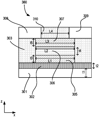
1. An integrated circuit comprising:
a gate dielectric;
a first layer adjacent to the gate dielectric;
a second layer adjacent to the first layer, the second layer comprising an amorphous material;
a third layer adjacent to the second layer, the third layer comprising a crystalline material; and
a source or drain at least partially adjacent to the third layer.