| CPC H01L 29/7869 (2013.01) [H01L 21/02554 (2013.01); H01L 21/02565 (2013.01); H01L 21/02631 (2013.01); H01L 21/823412 (2013.01); H01L 21/82345 (2013.01); H01L 21/823475 (2013.01); H01L 27/1225 (2013.01); H01L 27/1229 (2013.01); H01L 27/1233 (2013.01); H01L 29/66969 (2013.01); H01L 29/78603 (2013.01); H01L 29/78606 (2013.01); H01L 29/78618 (2013.01); H01L 29/78672 (2013.01)] | 24 Claims |

|
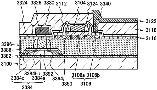
13. A semiconductor device comprising:
a first transistor, a second transistor, and a capacitor element,
wherein the first transistor is provided over the second transistor,
wherein a portion where one of a source and a drain of the first transistor is electrically connected to a gate of the second transistor is provided,
wherein data is written in the portion through the first transistor,
wherein the data is kept when the first transistor is in an off-state,
wherein a channel formation region of the first transistor includes a first oxide semiconductor layer,
wherein a channel formation region of the second transistor includes a second oxide semiconductor layer,
wherein the first oxide semiconductor layer includes a crystal whose c-axis is arranged perpendicular to a surface of the first oxide semiconductor layer,
wherein the second oxide semiconductor layer includes a crystal whose c-axis is arranged perpendicular to a surface of the second oxide semiconductor layer, and
wherein the capacitor element is electrically connected to the gate of the second transistor.
|