| CPC H01L 29/7869 (2013.01) [H01L 29/41733 (2013.01)] | 7 Claims |

|
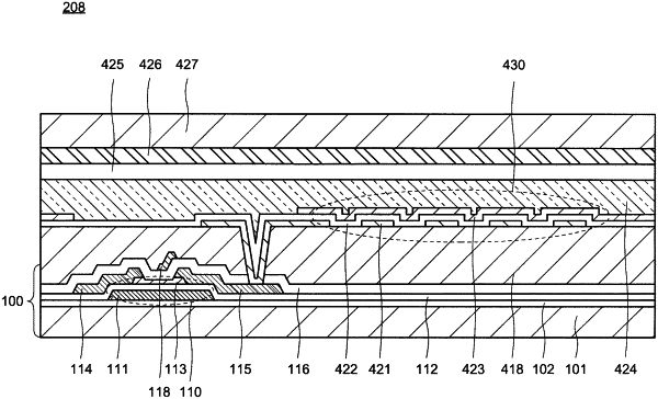
1. A semiconductor device comprising:
a gate electrode on a substrate;
a gate insulating layer on the gate electrode;
an oxide semiconductor layer on the gate insulating layer;
a source electrode and a drain electrode on the oxide semiconductor layer;
a protective layer on the source electrode and the drain electrode; and
a conductive layer on the protective layer;
wherein:
the source electrode and the drain electrode directly contact with a side wall and a part of an upper surface of the oxide semiconductor layer, respectively;
the protective layer includes a first silicon oxide layer and a first silicon nitride layer and overlaps the oxide semiconductor layer, the source electrode, and the drain electrode, in a plan view,
the first silicon oxide layer is in contact with the oxide semiconductor layer, the source electrode, and the drain electrode,
the gate insulating layer includes a second silicon nitride layer and a second silicon oxide layer,
the second silicon oxide layer is in contact with the oxide semiconductor layer, the source electrode, and the drain electrode,
the oxide semiconductor layer includes a first region located between the source electrode and the drain electrode, in a plan view,
the first region includes an overlapping region with the conductive layer and a non-overlapping region with the conductive layer, in a plan view, and
the conductive layer overlaps one of the source electrode or the drain electrode and does not overlap the other of the source electrode or the drain electrode, in plan view.
|