| CPC H01L 29/45 (2013.01) [H01L 21/28518 (2013.01); H01L 29/0673 (2013.01); H01L 29/0847 (2013.01); H01L 29/41733 (2013.01); H01L 29/42392 (2013.01); H01L 29/66545 (2013.01); H01L 29/66742 (2013.01); H01L 29/66795 (2013.01); H01L 29/7851 (2013.01); H01L 29/78618 (2013.01); H01L 29/78696 (2013.01)] | 10 Claims |

|
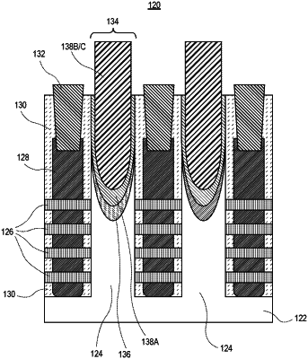
1. An integrated circuit structure, comprising:
a semiconductor structure above a substrate;
a gate electrode over the semiconductor structure, the gate electrode defining a channel region in the semiconductor structure;
a first semiconductor source or drain structure at a first end of the channel region at a first side of the gate electrode;
a second semiconductor source or drain structure at a second end of the channel region at a second side of the gate electrode, the second end opposite the first end; and
a source or drain contact directly on and in direct physical contact with the first or second semiconductor source or drain structure, the source or drain contact comprising a barrier layer and an inner conductive structure, wherein the barrier layer is a metal nitride barrier layer or a metal carbide barrier layer.
|