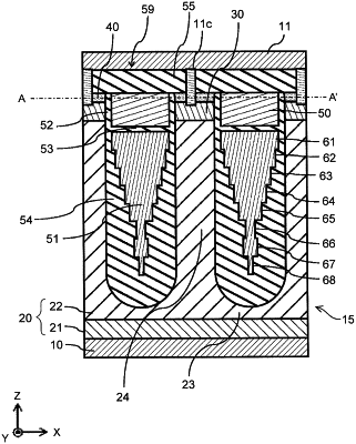
| CPC H01L 29/404 (2013.01) [H01L 29/407 (2013.01); H01L 29/4236 (2013.01); H01L 29/42368 (2013.01); H01L 29/7813 (2013.01)] | 11 Claims |

|
1. A semiconductor device, comprising:
a first electrode;
a second electrode;
a semiconductor layer that includes a first semiconductor region of a first conductivity type, a second semiconductor region of a second conductivity type, and a third semiconductor region of the first conductivity type, the first semiconductor region of the first conductivity type being located between the first electrode and the second electrode in a first direction from the second electrode toward the first electrode and electrically connected to the second electrode,
the second semiconductor region of a second conductivity type being located between the first electrode and the first semiconductor region in the first direction and being in contact with the first semiconductor region, and
the third semiconductor region of the first conductivity type being located between the first electrode and the second semiconductor region in the first direction and being in contact with the second semiconductor region;
a third electrode that is located between the first electrode and the first semiconductor region in the first direction and faces the second semiconductor region in a second direction intersecting the first direction;
a first insulating region that is located between the third electrode and the first semiconductor region, the second semiconductor region, and the third semiconductor region;
a second insulating region that is located between the third electrode and the first electrode;
a fourth electrode that is located between the third electrode and the first semiconductor region in the first direction and that has a plurality of portions consecutive in the first direction, the plurality of portions including a first portion that has a first width in the second direction,
a second portion that is adjacent to the first portion, located closer to the second electrode than the first portion in the first direction, and has a second width smaller than the first width in the second direction, and
a third portion that is adjacent to the second portion, located closer to the second electrode than the second portion in the first direction, and has a third width larger than the second width in the second direction; and
a third insulating region that is located between the fourth electrode and the first semiconductor region, wherein
the plurality of portions of the fourth electrode include a fourth portion that is adjacent to the first portion, located closer to the first electrode than the first portion in the first direction, and has a fourth width larger than the first width in the second direction.
|