| CPC H01L 29/401 (2013.01) [H01L 21/76897 (2013.01); H01L 29/41766 (2013.01); H01L 29/42316 (2013.01); H01L 29/42376 (2013.01); H01L 29/66462 (2013.01); H01L 29/7786 (2013.01); H01L 29/452 (2013.01); H01L 29/475 (2013.01); H01L 29/49 (2013.01); H01L 29/4983 (2013.01)] | 15 Claims |

|
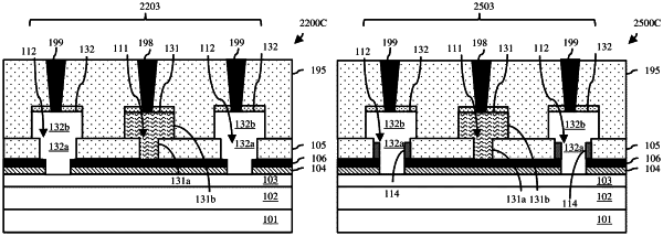
1. A structure comprising:
a stack of layers comprising: a channel layer; a barrier layer on the channel layer; and a dielectric layer on the barrier layer;
source/drain terminals; and
a gate terminal positioned laterally between the source/drain terminals,
wherein each source/drain terminal comprises: a first source/drain section within a source/drain opening that extends through the dielectric layer and the barrier layer to the channel layer; and a second source/drain section above the first source/drain section,
wherein each source/drain opening has a lower portion within the barrier layer and an upper portion within the dielectric layer and wider than the lower portion,
wherein the gate terminal comprises: a first gate section within a gate opening that extends through the dielectric layer and has a bottom above the barrier layer; and a second gate section above the first gate section and the dielectric layer, and
wherein the first source/drain section and the second source/drain section comprise a source/drain conductor material and the first gate section and the second gate section comprise a gate conductor material that is different from the source/drain conductor material,
wherein the stack of layers further includes a gate dielectric layer between the barrier layer and the dielectric layer,
wherein each source/drain opening further has a center portion within the gate dielectric layer between the lower portion and the upper portion, and
wherein the center portion and the lower portion have approximately equal widths.
|