| CPC H01L 27/156 (2013.01) [H01L 33/007 (2013.01); H01L 33/0093 (2020.05); H01L 33/0095 (2013.01); H01L 33/24 (2013.01); H01L 33/44 (2013.01); H01L 33/60 (2013.01); H01L 2933/0025 (2013.01)] | 19 Claims |

|
1. A method of manufacturing a light emitting element, the method comprising:
providing a semiconductor structure on a substrate, the semiconductor structure including different wavelength regions that emit light having different wavelength bands from each other;
after the semiconductor structure is provided, measuring the semiconductor structure to determine the different wavelength regions that emit light having the different wavelength bands from each other;
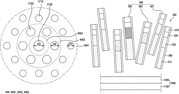
after measuring the semiconductor structure, forming nanopatterns spaced apart from each other on the semiconductor structure based on a respective wavelength region, the nanopatterns of each wavelength regions having different diameters from the nanopatterns of other wavelength regions, wherein a diameter of nanopatterns for each respective wavelength region is selected so as to cause different element rods formed from different wavelength regions to emit a common band of light; and
etching the semiconductor structure to form the element rods.
|