| CPC H01L 27/14645 (2013.01) [H01L 27/14621 (2013.01); H01L 27/14627 (2013.01); H01L 27/14634 (2013.01); H01L 27/14636 (2013.01); H01L 27/1464 (2013.01); H01L 27/14683 (2013.01); H01L 27/1469 (2013.01); H04N 25/79 (2023.01); H01L 27/14623 (2013.01); H04N 25/11 (2023.01)] | 19 Claims |

|
1. A solid state imaging device, comprising:
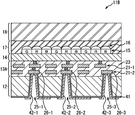
a semiconductor substrate that is provided with a pixel region on which a plurality of pixels is arranged in a planar manner;
a wiring layer that is laminated on the semiconductor substrate and is provided with a plurality of wirings connected to the plurality of pixels;
a support substrate that is bonded to the wiring layer and supports the semiconductor substrate,
wherein a plurality of electrode pads used to be electrically connected to an outside is arranged at positions overlapping the pixel region in the wiring layer when the semiconductor substrate is viewed in the planar manner;
a plurality of through-holes that are provided at positions corresponding to selected electrode pads of the plurality of electrode pads in the support substrate;
a through-electrode that is electrically and physically connected to a corresponding selected electrode pad at a bottom surface of a corresponding through-hole of the plurality of through-holes,
wherein the plurality of through-holes are each constantly tapered from an upper surface of the support substrate through a lower surface of the support substrate into the wiring layer such that openings of each of the plurality of through-holes at the upper surface of the support substrate are larger than openings of each of the plurality of through-holes at the lower surface of the support substrate; and
an insulation film formed on side surfaces of the plurality of through-holes extending into the wiring layer and on an entire surface of the upper surface of the support substrate except for where the plurality of through-holes exists.
|