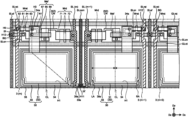
| CPC H01L 27/14607 (2013.01) [A61B 5/1172 (2013.01); H01L 27/14643 (2013.01); G06V 40/1318 (2022.01)] | 11 Claims |

|
1. A detection device comprising:
a substrate;
a plurality of photoelectric conversion elements provided to the substrate and each comprising a semiconductor layer having a photovoltaic effect;
a plurality of transistors provided for each of the photoelectric conversion elements; and
a plurality of signal lines, each of which is provided between the photoelectric conversion elements adjacent to each other in a first direction, extends in a second direction intersecting the first direction, and is configured to supply a signal to any one of the photoelectric conversion elements and the transistors, wherein
each of detection elements comprises one of the photoelectric conversion element and the transistors arranged adjacent to the photoelectric conversion element in the second direction,
a first signal line among the signal lines is arranged between the photoelectric conversion element of a first detection element and the photoelectric conversion element of a second detection element adjacent to one side in the first direction of the first detection element, and is coupled to the first detection element and the second detection element, and
a second signal line among the signal lines is arranged between the photoelectric conversion element of the first detection element and the photoelectric conversion element of a third detection element adjacent to another side in the first direction of the first detection element, and is coupled to the first detection element and the third detection element.
|