| CPC H01L 27/092 (2013.01) [H01L 21/823871 (2013.01); H01L 27/0207 (2013.01); H01L 27/0688 (2013.01); H01L 27/11807 (2013.01)] | 5 Claims |

|
1. A semiconductor integrated circuit device, comprising:
a plurality of cell rows each including a plurality of standard cells aligned in a first direction, wherein
a first cell row which is one of the plurality of cell rows includes a first standard cell having a logic function and a second standard cell having no logic function, the second standard cell being arranged at one or each end of the first cell row, wherein
the first standard cell includes
a first power supply line that extends in the first direction and is configured to supply a first power supply voltage,
a second power supply line that extends in the first direction and is configured to supply a second power supply voltage different from the first power supply voltage,
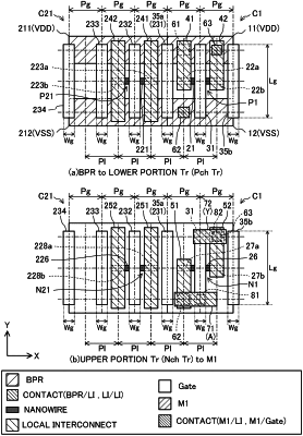
a first transistor that is a three-dimensional transistor of a first conductive type,
a second transistor that is a three-dimensional transistor of a second conductive type, which is formed at a position higher than the first transistor relative to a depth direction,
a gate line extending in a second direction perpendicular to the first direction and in the depth direction, which serves as a gate of each of the first transistor and the second transistor,
a first local interconnect and a second local interconnect extending in the second direction and connected to a source and a drain of the first transistor, respectively, and
a third local interconnect and a fourth local interconnect extending in the second direction and connected to a source and a drain of the second transistor, respectively;
wherein
the second standard cell includes
a third power supply line that extends in the first direction and is configured to supply the first power supply voltage,
a fourth power supply line that extends in the first direction and is configured to supply the second power supply voltage,
a first dummy transistor that is a three-dimensional transistor of the first conductive type, which is arranged in the depth direction in a same layer as the first transistor,
a second dummy transistor that is a three-dimensional transistor of the second conductive type, which is arranged in the depth direction in a same layer as the second transistor,
a dummy gate line extending in the second direction and the depth direction and arranged in the depth direction in a same layer as the gate line, the dummy gate line configured to serve as a gate of each of the first dummy transistor and the second dummy transistor,
a fifth local interconnect extending in the second direction, and arranged in the depth direction in a same layer as the first local interconnect and the second local interconnect, the fifth local interconnect connected to one of a source or a drain of the first dummy transistor, and
a sixth local interconnect extending in the second direction, and arranged in the depth direction in a same layer as the third local interconnect and the fourth local interconnect, the fifth local interconnect connected to one of a source or a drain of the second dummy transistor; and wherein
the sixth local interconnect overlaps the fifth local interconnect in plan view.
|